Power Calculations for IoT
In the lexicon of “on-trend” abbreviations, plain IoT – Internet of Things – has of late been supplanted by IIoT – for Industrial Internet of Things. This terminology sits alongside concepts such as Industry 4.0, and Smart Factory. A feature of the new industrial control environment is that it is proposed that field wiring for sensors and data collection points will be replaced, or at least supplemented, by wireless networks. The sensor nodes in question will be freely deployed wherever they are required, will be battery powered, and will operate at power levels low enough that they will function for many years without requiring any attention.
As with many engineering innovations, some aspects of the concept are not as new as might be supposed; the idea of wireless sensor networks has been around for at least 20 years: the IEEE’s working group on wireless personal area networks defined the 802.15.4 standard in 2003, and the first edition of the ZigBee standards – which spurred much of the initial thinking on the subject – appeared in 2004. Since then, many variants and additional capabilities have been layered on to the wireless part of the equation, and today’s designer has a choice of numerous open or proprietary schemes. Wireless connectivity, while being a key enabler, is only one of the areas where critical decisions are required: and the thread that will run through the complete design exercise is power.

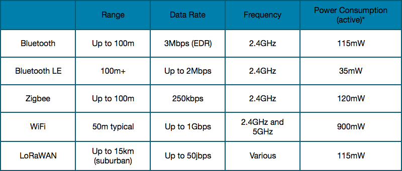
Table 1 – IoT Wireless Standards
*Power consumption is approximate values based on consumption of communications modules from TI, STMicroelectronics and Microchip at 3V.
Designing the power provision for such a sensor node presents a number of challenges. The power will come from a primary battery, or from a rechargeable component that might be a secondary battery, or a double-layer capacitor (“supercapacitor”), or a combination of those sources. In the latter case, recharging may be energy harvested from the environment – typically, a photovoltaic cell. In any of these cases, power will be a scarce commodity; a reserve that might be as small as a coin-cell or AA battery will have to operate for years without calling for a maintenance technician to make a replacement. Low-power IoT design takes place on timescale of years, rather than the hours associated with battery power in other contexts.
In a very real sense, certain parameters that will be listed in a specification and that may be part of warranted performance cannot be definitively tested. No one can afford to run a prototype for 10 years before placing a product on the market; therefore, claims such as “10-year battery life” will be, to some extent, based on extrapolation. It follows that the designer will have to have a high level of confidence in the measurements, calculations and predictions that underpin assertions about battery life.
The basic functional block comprises a sensor to measure some real-world parameter; some measure of signal processing and data pre-processing; and a communications link to convey measured data onwards in the overall control scheme. This node should wake up periodically, establish communications with its host, pass its data, and shut down again. Battery life is determined by the overall charge drawn; minimising that consumption in the long term means minimising it over each operating cycle. In many cases the node will have a very low duty cycle; a measurement that takes a few milliseconds may occur once per second, or per minute, or even longer. Therefore, the power used in standby can dominate the overall usage.
The total power used through each operating cycle is, clearly, the sum of the power drawn at every instant over that cycle; assuming a constant voltage, it is the area under the current vs. time graph. The arithmetic is simple; the implications for the architecture of the design can be less so.
Attention will naturally turn to the demands of the microcontroller around which the node will likely be constructed. If it spends, say, 99% of its time in a low-power state, then the fewer micro-Amps consumed in that state, the better. The MCU may offer a range of power-down states – deeper or less-deep sleep, with more, or fewer, peripherals active. Recovery to operating state will typically take longer from deeper standby states, and the power used in that wake-up must be accounted for in summing power over the cycle. Deeper sleep/microseconds spent in wake-up… at this point the designer might feel the need to set up a spreadsheet.
This line of thinking has to extend to every functional block in the IoT node’s design. Can the sensor itself be read immediately on power-up, or does it require time to stabilise? There may be amplification and filtering in the analogue domain, ahead of analogue-to-digital conversion: is it worthwhile in the overall power balance, to shut those elements down in the “sleep” part of the cycle? If it is, then is the settling time of op-amps or instrumentation amplifiers within the wake-up window of the MCU, or is a separate arrangement required? If gating power to individual blocks is thought worthwhile, then a power management IC may be required, which will enable detail control of power-up and power-down, but will add its own quiescent current contribution.
Returning to the starting point above, the communications medium of choice will also contribute to the power budget, and will have similar constraints. The RF link will take time and power to establish connectivity, before any data is transferred.
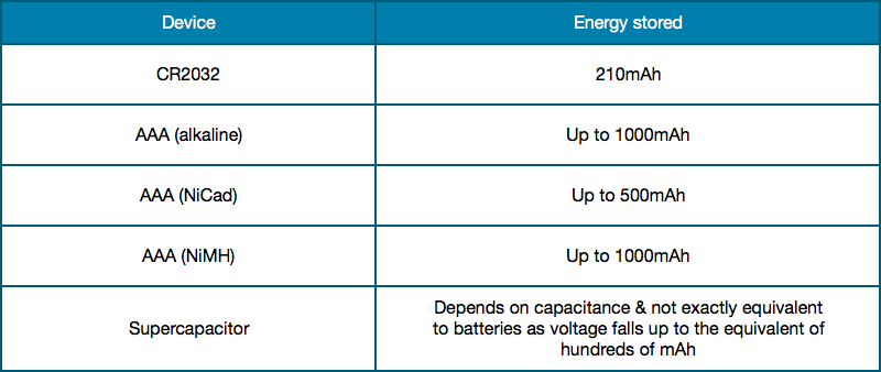
Batteries themselves become a significant part of the calculation process. The first requirement is that the battery must readily supply the peak power the applications will demand; and that once the average power has been determined and extrapolated to the target lifetime, that overall capacity is adequate. The ubiquitous CR2032 has a nominal capacity of 210 – 220 mAh; if a microcontroller is to run in standby (only) for 10 years, it would therefore need to draw 3µA (220mAh/87600hours) or less. That simple calculation does not take into account the cell’s self-discharge rate; Energizer, for example, specifies its CR2032 as losing around 1% capacity per year. Also, the nominal capacity is specified at a particular load – 240mAh into 15kΩ to a 2V end-point, in the case of the Energizer cell (or 200µA when ‘fresh’). The actual capacity obtained will vary with load, in general reducing at higher currents. One area in which industry trends are helpful is in the specification of battery (primary cell) shelf-life; today’s branded alkaline or Li-MnO2 cells are sold, even in retail, as “holding power for 10 years,” and with a decade’s use-by coding. In the past, even obtaining batteries that guaranteed usability after 10 years could be problematic.

Table 2 – Energy Storage
Similarly, although use of energy harvesting with some form of rechargeable power reserve might lessen the need to minimise every power-consuming function, product life of a decade or more is likely mean that rechargeable cells will see some reduction in capacity compared to their performance when new. Both primary and secondary cells should also be conservatively rated as they are to be used in challenging conditions (e.g. sustained low temperatures).
Although extended battery life is planned, the low power IoT node design must be able to notify its host if its power source does fail. If the analogue circuitry has the spare capacity, this might be as simple as a comparator, or an unused op-amp, detecting the voltage rail falling below a pre-set level; or, at the expense of consuming a few more processor cycles, making that measurement with an ADC input. In either case the trip point would be set so that sufficient power remained to send a suitable message.
It is around the microcontroller power calculations that most effort is likely to be expended, however. Key metrics that guide device selection will include the MCU’s current consumption (in µA/MHz); a suitable mix of peripherals, headed by an A/D converter of appropriate performance; and the complexity of the compiled code (number of cycles to be executed from wake-up to shut-down).
Microcontroller Selection
One of the first choices to be made will be between 8, 16, or 32-bit. An 8-bit device might be expected to offer lowest power and in many cases, that will be true. For example, and looking across Microchip’s PIC ranges, there are 8-bit PIC18F "K42" XLP products that consume 45µA per MHz (up to 64 MHz) when active (https://www.farnell.com/datasheets/2297480.pdf); a 16-bit device, the PIC24FJ256GA412/GB412 consumes 160µA/MHz; while the 32-bit PIC32MX consumes 250µA/MHz. As might be expected, higher power comes with higher performance. Even within the 8-bit device, there are multiple options to explore to manage power, including three separate power-saving modes for the core, and a range of XLP (eXtreme Low Power) features that set, for example, timer and oscillator parameters. Included in a list of peripherals headed by a 12-bit ADC, are four Configurable Logic Cells that can implement simple combinational/sequential logic functions. This seemingly minor addition to the specification could well save an external package, performing some logical decision making without, or prior to, waking the core.
A wider bus-width device might be preferred if, for example, the sensor input is of high precision and digital filtering is required: this could rapidly ramp up the number of processor cycles required in a smaller core, with the result that a higher-performance device could complete the task much faster, and shut down to standby sooner.
Microchip also offers the SAML21/22 32-bit processors (ARM Cortex-M0+ parts from the company’s Atmel acquisition, running at up to 48 MHz) which consume just 32µA/MHz, so if these meet the application needs (they have lower peak performance than the PC32MX) then they present a good choice, especially if the design team already has ARM development experience.
Texas Instruments has a long-established track record of very low power MCUs in the MSP430 series, and continues to add to the range. The ability to “tune” an application for power is illustrated by features of the MSP430FG662x and MSP430FG642x devices, that have, in addition to Active mode; a Standby mode, where data is retained in RAM and the system can wakeup quickly; a shutdown mode, with the RTC (real-time clock) continuing to operate; and a very low power shutdown mode.
At 3V, the active mode consumes 250µA/MHz (and the device can run up to 20MHz, for a current consumption of 5mA), the standby mode 3.4µA, and the shutdown modes 0.9µA and 0.2µA respectively. The most dramatic power saving is from active to standby, when power consumption can be reduced several-hundred-fold. However, the difference between standby and shutdown can be very important: at one level it is a further, almost four-fold, reduction in power – but it also allows the real-time clock to keep running, providing an essential feature to generate the “wake-up” command. Also in the data sheet is the time to wake from the standby condition, to full operating status; in this case, 3µs. During its “wake-up” period, the MCU will run at its “fully-active” current level. Waking the same (´662x) device from shutdown rather than standby takes 2ms , not 3µs. The designer’ calculation therefore has to balance the time spent in the “off” part of the duty cycle with the extra power need to return, to determine if stepping down to the deeper level is worthwhile.

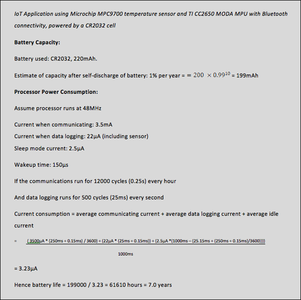
Figure 1 – Example battery life calculation for an IoT application
The paragraphs above pre-suppose that if a wireless connection is envisaged, then a stand-alone RF module, or IC, will be part of the design. That will come with its own data-sheet figures for start-up time and power, and the current drain to be expected when in full operation – which must be added to the overall power budget, for the period of the duty cycle that the RF is ‘on’. Farnell lists a wide range of modules for ZigBee networks, for proprietary IEEE 802.15.4 operation, and for other standards. To select just one as an example of Zigbee power demands, Silicon Labs’ ETRX35x-LRS is a module based on a single-chip design, that wakes from a deep-sleep state in 100µs, uses around 30mA in receiver mode and from 50 – 140mA in transmit, depending on output power. From those figures it is immediately clear that minimising RF (particularly transmit) ‘on-time’ is key to keeping the overall power budget in check.

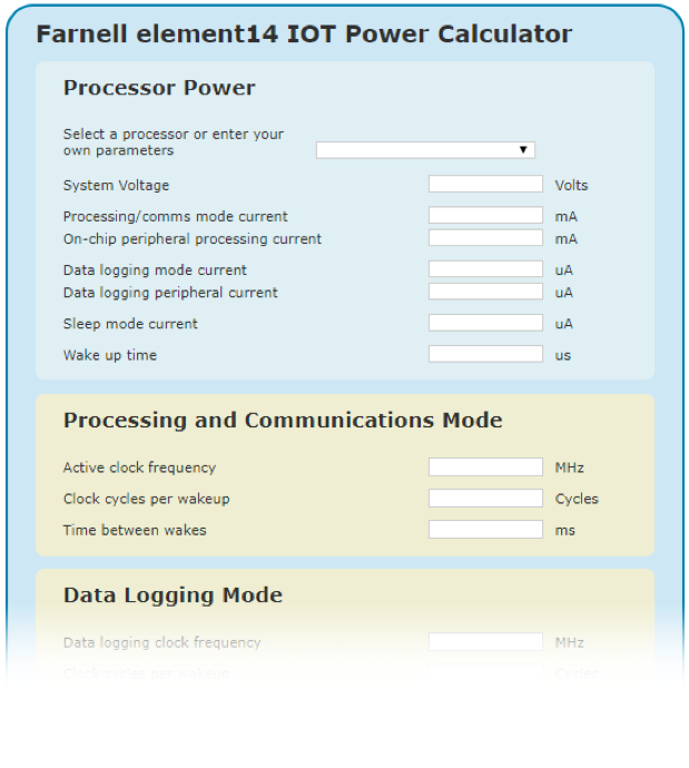
Figure 2 – IoT Power Calculator
Yet another variation is to configure a design using a single-chip microcontroller device with integrated RF functionality, in which the MCU core has sufficient “headroom”, or capacity, to host the measurement and reporting applications code, as well as to run the communications stack. An example from NXP’s range is the JN5179 ZigBee and IEEE802.15.4 Wireless Microcontroller that comes with 512 kB of Flash memory, and 32 kB RAM. This IC has an ARM Cortex-M3 core, with programmable clock speeds, and an RF transceiver that is configurable for the generic link operation, or for ZigBee compliance. The radio in this example powers-down to 100 nA consumption; the MCU has a 10-bit ADC, and adds features such as integrated battery voltage monitoring.
Other RF strategies may be applied as circumstances demand, but will impose their own power specifications. Where the operating environment already has WiFi (IEEE802.11/b/g/n) coverage, that may present a convenient means of collecting field data – but at a power cost. Taking another Silicon Labs product, based around one of its Gecko chips (again, an ARM Cortex-M3 core), the WGM110 , the data sheet shows transmit current of 261 mA, receive current of 8mA and ‘idle’ current of 2.2mA – with a 22µA deep-sleep figure. In a different environment, where long range is needed, the LoRa standard may be applicable.
System partitioning as the above examples illustrate, can hold the key to achieving battery life targets. This holds true at the front end of a sensor node. Some systems might use an analogue temperature sensor, such as Texas Instruments’ LMT84-Q1 1.5V-capable, 10 µA analogue output temperature sensor. This is a very low-current device, at 8.1µA. It has to be polled by the microcontroller and the analogue measurement converted by the MCU’s ADC, all adding to the “active” current consumption. Using a digital temperature sensor such as (also from TI) the TMP102 will remove the need for the ADC to be used in the MCU, but more importantly it can continuously monitor the temperature and then send an alert signal to wake the CPU if the temperature is outside a pre-set range. This can significantly reduce the power consumption by allowing the CPU to remain in sleep mode for a longer period of time, while continually monitoring the temperature.
If the designer opts for a high level of power control, a power management IC (PMIC) comes into play. These exist in almost limitless variations from numerous manufacturers; one example intended for exactly the primary-battery-powered, long-lifetime application envisaged here, is Maxim Integrated’s MAX14720 . For non-rechargeable battery (coin cell, dual alkaline) applications where size and energy efficiency are critical. It integrates five discrete devices; power switch, linear regulator, buck regulator, buck-boost regulator, and monitor. A programmable power controller configures the part either for use in applications that require a true off state or for always-on applications. This controller provides a delayed reset signal, voltage sequencing, and customized button timing for on/off control and recovery hard reset.
An additional feature is a battery “seal” - implemented electronically – that completely disconnects the battery prior to initial commissioning. This allows products to be shipped with battery included – a less obvious benefit is that the manufacturer can thereby ensure that the battery fitted when the IoT node is put into service, is of a quality that matches the decade-long lifetime aspiration.
Power Calculations for IoT. Date published: 15th March 2018 by Farnell element14