How to improve analog to digital converter accuracy
The accuracy of an ADC (Analog to Digital Converter) exhibits how close you are to represent the true signal in your measurement. It is determined by the DC specifications for gain, offset, and linearity and is affected by parameters associated with voltage source, I/O switching, PCB layout and analog source impedance.
What's important about accuracy, is that it can tell us the types of errors we see in our measurement. To increase the ADC accuracy, you need to reduce the effects of the ADC-related errors and minimise ADC errors related to the external environment. The ADC accuracy cannot depend upon the ADC performance and features alone; it depends upon the overall application design around the ADC.
To increase ADC measurement accuracy:
a. Reduce the effects of the ADC-related errors: The accuracy of ADC impacts the overall system quality and efficiency. To improve accuracy, you need to understand the errors associated with the ADC and the parameters affecting them. The ADC errors related to itself include: offset error, gain error, differential linearity error, integral linearity error, and total unadjusted error. The errors can be compensated for by using the ADC self-calibration feature or by using software-based techniques.
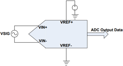
b. Avoid using a power supply (Vcc) as the reference voltage (Vref): The ideal ADC produces a digital output as a function of the analog input voltage and the voltage reference input (Figure 1). For better ADC measurement accuracy, you do not want Vcc as Vref as it can adversely affect the output with the line, load, and temperature drift. There are typically other options for ADC Vref voltage- either utilising a built-in Vref voltage provided by ADC manufacturers, or to use an ADC with an external Vref with a dedicated Vref pin.

Figure 1: ADC measurement circuit
c. Eliminate the analog-input signal noise: Small but high-frequency signal variations can result in big conversion errors during the sampling time of ADC. As a consequence, the conversion results of the ADC are not accurate. Eliminate the analog-input signal noise by using the averaging method or adding an external filter (Figure 2a).

Figure 2a: External RC filter to eliminate analog input noise. Figure 2b: Analog source resistance.
d. Analog source resistance match: The impedance of the analog-signal source or series resistance (RAIN) between the source and the pin causes a voltage drop across it because of the current flowing into the pin (Figure 2b). The charging of the internal sampling capacitor CADC is controlled by switches with resistance RADC. The time required to charge the hold capacitor increases with the addition of source resistance (RADC). Always ensure that the analog signal source resistance is within the ADC specification. The software-based approach can configure the sampling time to be longer than the settling time.
e. Minimise I/O pin crosstalk: Switching the I/Os may introduce some noise in the analog input of the ADC due to capacitive coupling between I/Os. Crosstalk may be introduced by PCB tracks that run close to each other or that cross each other. The noise produced by crosstalk can be reduced by shielding the analog signal by placing ground tracks across it. Figure 3 shows the recommended grounding between signals.

Figure 3: Recommended grounding between signals.
f. EMI-induced noise reduction: Electromagnetic emissions from the nearby circuits may introduce high-frequency noise in an analog signal because the PCB tracks may act as an antenna and impact the analog signal input line. Reduce EMI noise by using proper shielding and layout techniques.
g. PCB layout recommendations: The PCB layout recommendations include separating the analog and digital layouts, separating the power supplies for the analog and digital circuits, component placement and routing. It is recommended to use different planes for analog and digital grounds (Figure 4). This avoids tracks crossing each other and also avoids introducing high-frequency noise in analog signals because of coupling.


