Extending the battery-life of an IoT BLE device
The Internet of Things relies on edge devices that collect and send data to the cloud. Usually these devices are small, battery-powered and require little maintenance. Users have high expectations –of what the device will achieve and how long the battery will last. Developers now have many goals but making sure it consumes as little energy as possible is certainly one of them – to give the user an optimum battery lifetime.
In this article, we take a closer look at the L-Tek FF1502, a Bluetooth Low Energy (BLE) based sensor tag which operates as a broadcaster, i.e. beacon. Beacons are typically low power devices, which sleep most of the time and wake-up briefly to broadcast a message to nearby portable electronic devices (such as mobile phones for example). We’ll show how to optimize the battery lifetime of an application running on the beacon by using the ULINKplus debug adapter that enables high-precision power analysis together with Arm® Keil® MDK
Arm Keil MDK and ULINKplus
Keil MDK is the complete software development solution for Arm-based microcontrollers and includes everything required to create, build, and debug embedded applications. Keil MDK is a powerful, yet easy to learn and use development system.
The µVision IDE, that is part of Keil MDK, offers unique debugging capabilities when used in conjunction with the ULINK family of debug adapters. The newest member of the family is the ULINKplus, which combines isolated debug connection, power measurement, and I/O for test automation. It gives visibility into function, timing, and power consumption of embedded applications.
ULINKplus is easy-to-use and connects to Arm Cortex-based devices. It supports all classic debug features such as simple and complex breakpoints, SWV trace, and even multi-core debugging. Together with Arm Keil MDK, the Event Recorder and Event Statistics profile applications for timing and energy consumption. And the new System Analyzer in µVision correlates power consumption with events, threads, interrupts, and variable changes, making it even easier to optimize power hungry code.
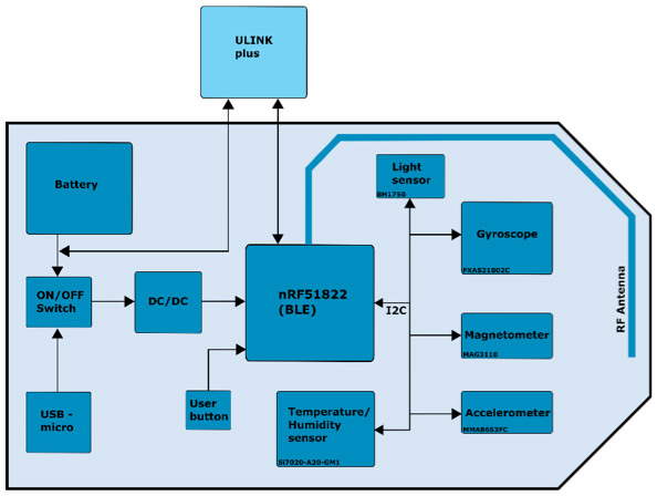
The L-Tek FF1502
The L-Tek FF1502 has a small form factor and an XBee compatible pin-out that makes it a perfect building block for IoT applications. The device can be powered by a single CR2032 coin cell battery or via USB. It is based on the Nordic nRF51822 microcontroller (Arm Cortex-M0-based) with an integrated Bluetooth radio. Various sensors are connected to the microcontroller via I2C:
- temperature & humidity (Si7020-A20)
- light (BH1750)
- accelerometer (MMA8653FC)
- gyroscope (FXAS21002C)
- magnetometer (MAG3110)
The USB connector and CR2032 battery are connected to a DC/DC switch which provides power to the complete circuit (including the capacitor network).
The application
During run-time, the application sleeps most of the time with the MCU and sensors all being in low power mode. Every ten seconds, it wakes-up periodically and reads the sensors (temperature, humidity and light). Then, the sensor data is broadcasted via BLE and the device goes back to sleep again.
Reference Design
In the following, the original hardware and software design is called "reference design". The initial power measurement shows the following power intensive cycle (with a duration of 51 ms) which is repeated periodically (every ten seconds):
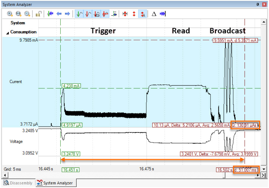
According to µVision’s System Analyzer, the total electrical charge for the active cycle is:

The cycle can be divided into the following phases:
- triggering sensors over the I2C bus to start a single measurement
- reading sensor data over the I2C bus
- broadcasting the sensor data over BLE
- sleeping before and after
Triggering sensors
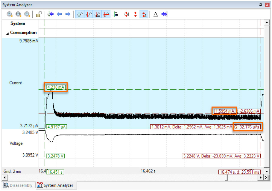
Sensor measurement is triggered by issuing commands over the I2C bus and waiting until the data is ready. There is a 4.2 mA current spike at the beginning, when the MCU is running at full speed, communicating over I2C. This is expected as 4 mA is the typical MCU run current (according to the MCU's datasheet). After that, the MCU will wait for around 20 ms in low power mode. The expected current is around 300 µA which is the current required by the sensors during measurement (according to the sensor datasheets).
Therefore, the actual current of around 1.6 mA seems to be too high and should be investigated. The total electrical charge for triggering sensors is:

Reading sensor data
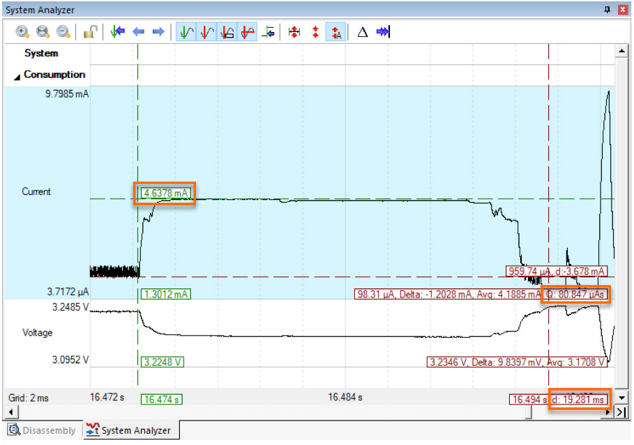
Sensor data is read over I2C in polling mode. The MCU is active during the entire read process, which matches the measured average current of 4.6 mA. However, the whole read process takes about 19 ms, which seems to be long due to the small amount of executed I2C transfers.
On this basis, the read time needs to be investigated and an alternative to polling mode, such as event driven I2C communication should be considered.
The total electrical charge for reading sensors is:

A similar analysis can be done for sleep and the broadcast phase. However, as the broadcast phase is totally dependent on the radio firmware that is provided by the silicon supplier, there is no room for optimization.
Software investigations
After checking the different execution phases of the application, a couple of problems can be identified that required further investigation:
Unexpected high current during sensor trigger phase
Due to a bug in the software, an extra I2C write operation is issued which leads to an increase in the sensor current. Removing that code, the current drops from around 1.6 mA to the expected 300 µA during the sensor trigger phase. This reduces the electrical charge for the Triggering Sensors phase from 33 µAs to 6.5 µAs.
Long I2C transfer time during sensor read phase
The long I2C transfer time is caused due to the same software bug which increases the sensor current as well as causes I2C clock stretching by the sensor. The read phase is drastically shortened after removing the extra I2C write. This also significantly reduces the electrical charge for the Reading sensor data phase from 84 µAs to just 8.3 µAs.
Event driven I2C transfers vs. polling mode
Using event driven I2C transfers enables the MCU to go to sleep while waiting for the I2C transfer to complete (rather than running at full power while polling the I2C transfer state). This further reduces the required current during the Reading sensor data phase. However, the impact is small due to the already shortened I2C transfer time.
Redesigned software
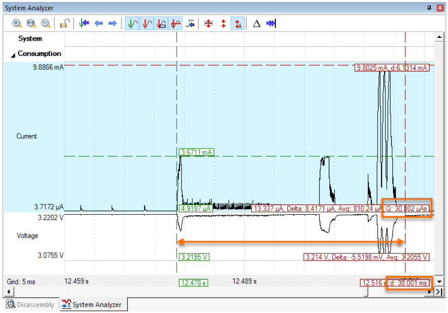
The software of the reference design was updated based on findings from the software investigations. The I2C write operation bug was fixed and event driven communication was introduced. The newly measured power profile shows the updated power intensive cycle - now much shorter at 38 ms.
Hardware investigations
The sleeping phase measurements show an average current of 13.6 µA, which is higher than the expected 9 µA (based on the datasheets). To isolate the problem, the application is modified so that the MCU immediately enters low power mode without any other functionality (no sensor read or BLE broadcast). This results in current pulses with an average 4.4 ms period (same as in the application). The residual 5 µA current still exists.
Hardware redesign
The hardware design is analyzed to determine the source of the additional 5 µA current consumption. The analysis shows that this is caused by the reverse current of the protection diode D2.
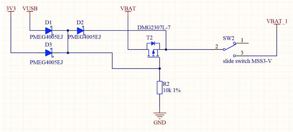
Replacing the original D2 diode PMEG4005EJ with PMEG6010CEH almost eliminates this current ( less than 0.2 µA) and the overall current in sleep mode reduces to 8 µA.
Battery life
The FF1502 runs from a CR2032 battery with the following capacity:

The FF1502 samples and broadcasts sensor values every 10 seconds. To calculate the total energy consumption, the Qref_active can be divided by this broadcast interval, to get the average current consumed. Adding the sleep mode current gives the total current consumption.

Reference design

Redesigned software and hardware

Doubling battery life
Optimizing embedded applications for overall efficiency should be an integral part of the development process as it is important to understand how peripherals, software algorithms, and power saving modes work together. To simplify it we developed ULINKplus, a universal debug and trace adapter that includes power measurement. Together with Keil MDK, this debug unit gives you unparalleled insight into the operation of your microcontroller applications. It shows you which parts of your application code consumes more power and helps you to verify the usage of low-power configurations.
ULINKplus is designed for software engineers and is easy to connect to target hardware. Compared to oscilloscopes, it does not require complex configuration settings and shows a higher dynamic range that allows you to spot small current differences. It even correlates the power measurement with the program execution when using trace or event annotations.
In this example, we demonstrated that reducing the overall energy used by an existing application through improvements to software and hardware is highly achievable. In fact, the original battery life was more than doubled as a result of optimization. Learn more about ULINKplus on www.keil.com/ulinkplus
Extending the battery-life of an IoT BLE device. Date published: 15th June 2018 by Farnell element14